
Semiconductor R&D and quality control
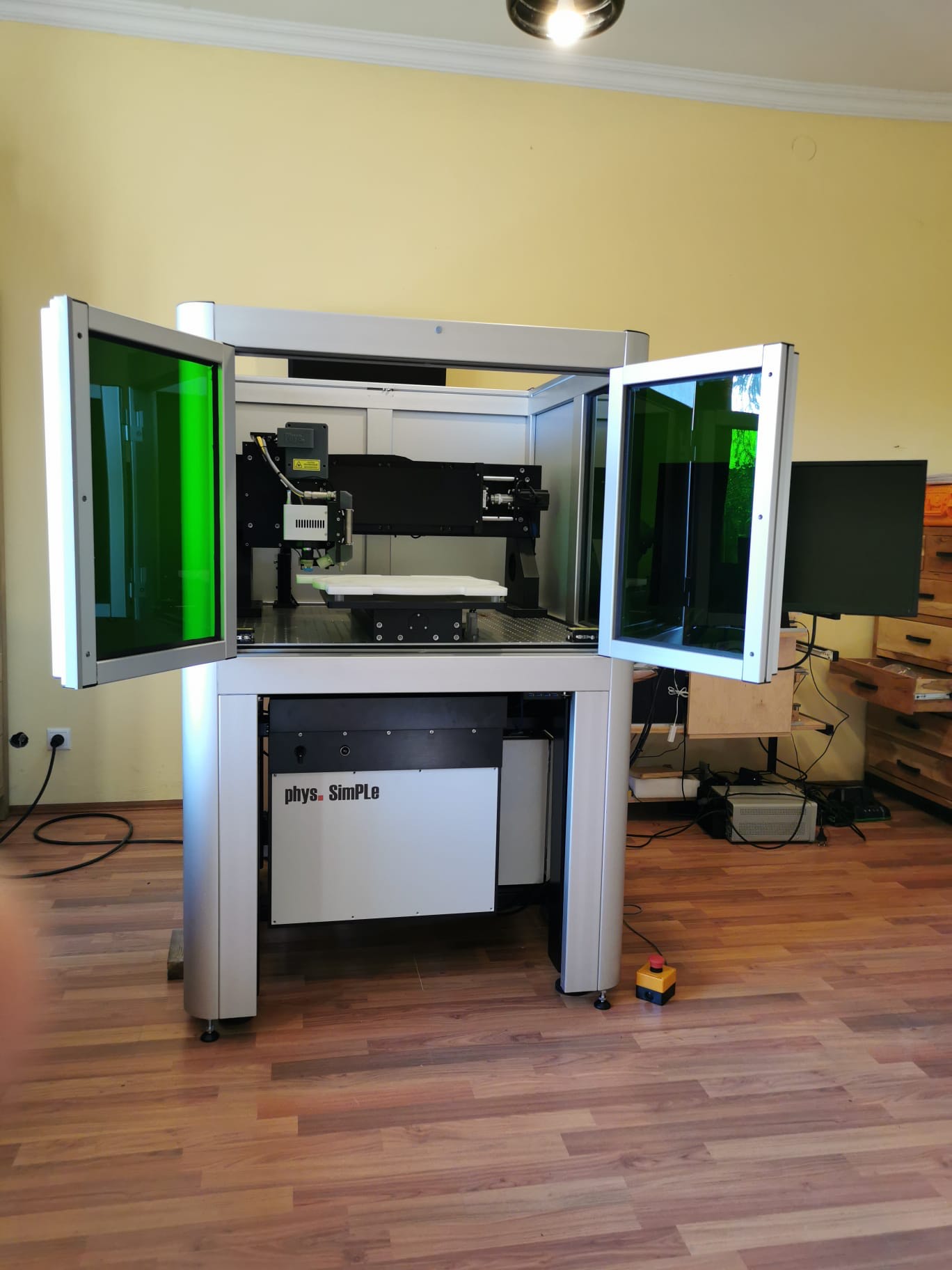
Semiconductor wafer inspection platform
A unified measurement environment connecting precision equipment, image acquisition and custom analytics.
 Project
The challenge
Semiconductor inspection equipment needs to coordinate precision hardware, measurement sequences, image acquisition and analysis while giving engineers a clear view of the results.
Our contribution
Symmetrix developed an integrated measurement-software environment for wafer inspection. The system brings equipment control, acquisition and custom analytics toolchains into one operator workflow. Wafer scans reveal structures and defects that are not apparent on the matte-grey surface to the naked eye.
Delivered capabilities
- Measurement-sequence and equipment integration
- Image acquisition and wafer visualisation
- Custom measurement and analytics toolchains
- Operator-focused Windows desktop workflow
- Support for semiconductor testing and quality-control processes